The first step in the process of Laser Dicing is to determine which type of dicing process will best suit your needs. There are three main types of dicing: Full-thickness, Stealth, and Plasma. The types of dicing methods vary greatly, but there are certain things that are common to each. Using the correct technique will produce the best results. In addition, a good practitioner should be able to explain the process to you so that you can make an informed decision.
Full-thickness laser dicing
The method involves the use of a high-power laser to shave away device layers, while the backside of the wafer is left intact. Full-thickness laser dicing is different from surface scribing. The backside of the wafer is mounted using a dry film vacuum lamination process. The wafer is then placed onto a laser scribing stage, and the laser beam is focused down into the trench. The disadvantage of typical laser processing is the damage to the dicing tape and the contamination of the die sidewalls. However, embodiments of this technology can overcome these issues.
A typical process tool comprises a factory interface 602, multiple loads locks 604, and a cluster tool comprising one or more plasma etch chambers. A laser scribe apparatus 610 is coupled to the factory interface. These processes may be performed simultaneously, or in succession. The dicing process may include multiple stages. One approach uses a laser scribe to cut through a layer of silicon, while another uses a plasma etching technique.
Stealth dicing
As memory device packaging moves toward die stacking technology, the process of wafer dicing is becoming increasingly critical for semiconductor yields. Laser Stealth dicing is an emerging technology that uses laser irradiation to form a modified layer inside the wafer without damaging the surface. This technology uses a different type of laser than the existing stealth dicing process, which requires ultrashort pulse lasers and is costly.
The laser is focused on the bulk material, so the area of damage is constrained. In this way, the laser will not generate a filamentation along the entire thickness of the quartz plate. However, the heat generated by the laser will accumulate. This mechanism will result in a crack generation. As a result, the cracks will propagate along the path of the laser. This will eventually affect the whole thickness of the quartz plate.
The advantages of Laser Stealth dicing include its high accuracy and clean-cut edges. Unlike blade dicing and laser ablation, the process of Laser Stealth dicing is a single pass and does not involve any chemical agent or external tensile stress. The laser is controlled by a number of parameters including pulse overlap and repetition rate. Optical microscopy and optical profilometry are used to assess the quality of the cuts.
The process of Laser Stealth dicing involves a laser source 380 that focuses an infrared light beam. The beam then travels to a depth inside substrate 210, and the second main surface 214 is located opposite to the first main surface. The distance L between the two surfaces can be reduced in order to speed up the process. This method of dicing is more efficient than conventional dicing but requires a high-quality substrate.
In addition to the high precision, Laser Stealth dicing is a cost-effective alternative to traditional lithography. The technique uses ultrashort pulses to cut quartz plates. The main factors influencing the efficiency and quality of the cut are pulse energy, repetition rate, and side wall generation. The advantages of Laser Stealth dicing over other methods of dicing are outlined below. If you are interested in using Laser Stealth Dicing, be sure to explore these advantages.
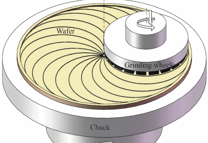
The process is capable of cutting a wide variety of materials and shapes. The laser beam’s kerf width is between two and fifteen microns. Silicon is the most common material for dicing, and the most efficient lasers have a high NA focus lens group. This high-NA lens can form a modified layer within the wafer. If you’re in the electronics industry, this process could be your best bet for a profitable business.
Click here to read more: https://www.stealthdicing.com/about-gdsi/
Plasma dicing
Plasma dicing is a promising new technology that replaces traditional blade dicing. It is an environmentally friendly process that involves no contact with the silicon and doesn’t produce heat-affected zones. Plasma dicing creates a higher break strength than laser or blade dicing, which makes it a better option for high-stress die. It also requires less downtime than other dicing methods. If you’re wondering whether plasma dicing is the right technology for your product, keep reading.
Although plasma dicing is very effective, it also has some limitations. This technology is relatively expensive to implement, and it may require the use of a standard lithography operation. In addition, it may have high throughput limitations and production issues with commonly encountered metals. If you’re looking for a new solution to dice wafers, plasma dicing with a laser may be a good choice for you. This article describes the process and what it can do for your company.
As chips become increasingly smaller, this process presents a number of challenges. Traditional dicing techniques use a blade saw, resulting in high material loss and mechanical damage. Plus, the traditional dicing process takes too long. Plasma dicing is a better solution because it uses dry etching, which eliminates contamination and dies stress. Additionally, narrow dicing lanes increase wafer dicing throughput. Furthermore, with smaller die sizes, you can design more chips on a wafer. By utilizing a plasma dicing system, you can achieve high-quality semiconductors.
While plasma dicing has a high cost, the process is much more efficient than blade saw dicing. It also produces less heat, making it an attractive alternative to conventional blade saw dicing. It’s worth considering for ultrathin dies. These dies can be produced cheaper and have more consistent quality. With the proper application, this process can help you get the best quality products without breaking the bank. If you are looking for a laser-dicing San Jose process, this will be a great choice for you.
This hybrid dicing process combines a laser scribe and a plasma etch. First, the laser scribe removes the mask layer. Afterward, the plasma etches chamber etches the bulk of the wafer. This process may be done on single crystalline silicon or a substrate. It depends on your needs and your budget. When it comes to plasma dicing, the cost per die is low and you can get a good yield.
The kerf width ranges between 50-100 microns. The kerf width is important because it will help separate adjacent chips. Also, it will eliminate test patterns. A major focus of plasma dicing is to get a delamination-free process. This way, you can be sure that the final product will have a high quality. If you’re wondering how to improve the quality of the product, this article is for you.
Thanks for visiting blogspinners